Where Is Inkjet Heading Next? Findings from LOPEC 2026
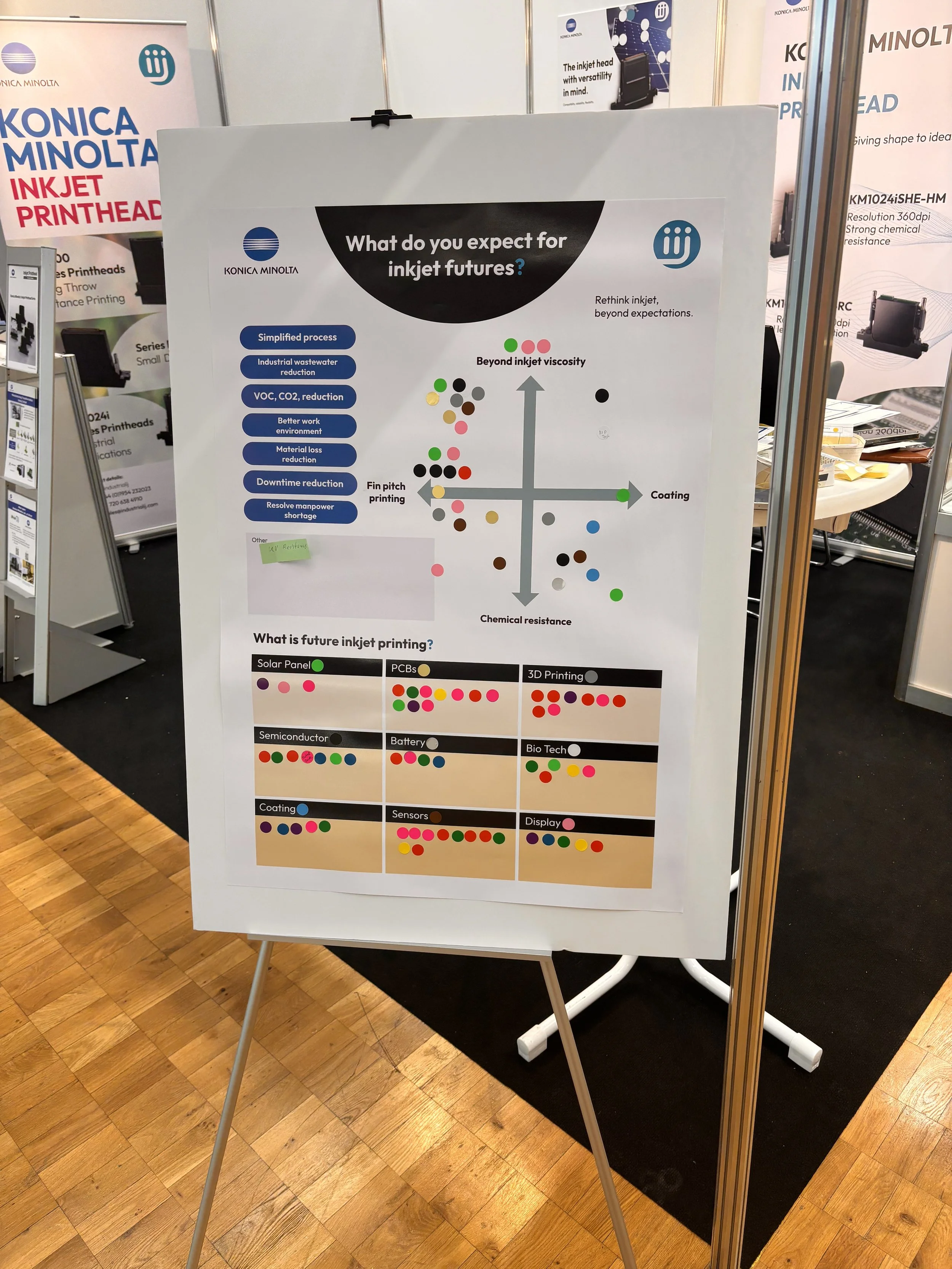
While walking around the hall of LOPEC, we stumbled across Konica Minolta’s stand that had a simple but telling feature: a large board asking, “What do you expect for inkjet futures?” Visitors were given coloured stickers and invited to place them wherever they thought inkjet was heading.
By the end of the show, the board was covered in dots.
Each cluster showed where engineers, materials scientists and system developers believe inkjet is moving. Some gravitated towards higher-viscosity materials and coating applications. Others leaned towards chemical resistance or finer pitch printing. Further down the board, more dots gathered around solar panels, PCBs, 3D printing, semiconductors, batteries, sensors and displays.
The density of those dots told its own story. Inkjet is expanding into areas that sit well beyond traditional print markets.
For the FuturePrint audience, particularly those focused on packaging, labels and industrial print for advanced manufacturing, these adjacent applications are worth watching closely.
The findings from LOPEC 2026
Printed electronics
One of the most active areas is printed electronics. Inkjet is being used to deposit conductive inks for flexible circuits and PCB structures. The precision required is high, and the tolerances are tight. What stood out at LOPEC was how mature some of these applications now look.
That progress matters for packaging. Smart labels, embedded antennas and printed sensor elements rely on the same core capability: controlled material placement at small scales.
Solar and energy devices
Inkjet is also being used in solar panel production to apply functional layers and conductive materials. The goal is accurate placement and efficient use of expensive materials. Similar work is happening in battery research, where active materials are deposited in defined patterns.
The chemistries involved are different from packaging inks, but the engineering challenges are familiar. Handling demanding materials while maintaining reliability pushes printhead design and fluid management forward.
Semiconductor processes
In semiconductor manufacturing, inkjet is used to place specialised materials with precision. The expectations around consistency and durability are high. Developments in this environment tend to raise the bar for hardware robustness and material compatibility more broadly.
The improvements made in these demanding sectors often feed into industrial systems used elsewhere.
3D printing and additive manufacturing
Material jetting systems use inkjet-style deposition to build objects layer by layer. Instead of decorating a surface, the droplets form the structure itself.
At LOPEC, additive manufacturing appeared alongside a range of other advanced manufacturing applications where inkjet is being adapted to deposit functional materials with precision. These systems are often used for electronics, prototyping and specialist components where controlled material placement is critical.
For those working in industrial print, it is another reminder that inkjet is increasingly being explored as a manufacturing tool as well as a decoration technology.
Functional coatings
Another area gaining attention is digital ‘inkjet’ deposition of functional coatings. Instead of blanket coating a surface, material can be applied precisely where it is needed. This supports more complex surface performance and more efficient material usage.
For packaging and labels, this opens up possibilities around targeted barrier layers or specialised surface treatments applied digitally.
Sensors and bio-related applications
Inkjet is also appearing in the development of compact sensors and certain bio applications. The ability to deposit small volumes of functional material in controlled patterns supports the creation of lightweight sensing devices.
For packaging, this connects with traceability and condition monitoring, areas that continue to evolve.
That board at LOPEC, covered in coloured dots, captured something useful. It showed where the technical community sees momentum building. The clusters weren’t random. They reflected real projects and active development. So, from our side of the industry, it seems watching where those dots gathered will help frame where industrial inkjet could move next.
Thank you to Konica Minolta for their permission to use the image.